Signal Integrity

Signal Integrity testing

Poster: Signal integrity eye test

Contact us

Signal Integrity measurements

Signal Integrity; how close is the signal to ideal, in terms of all measurable parameters in both the frequency and the time domain? As signaling rates increase and voltage swings decrease, the jitter becomes an increasingly significant percentage of the unit interval, and acceptable noise levels constantly lower. For a communication device, testing the quality of the signals output from the device, and signals that have been input at interfaces will detect signal integrity problems. If the signal quality must be improved, waveforms in both the signaling and the clock circuits of the device must be analyzed. Other potential causes of signal integrity problems are the device power circuits, and internally caused EMI.

Interfaces

For any signal communication device there are descriptions of the physical qualities of the I/O, and the acceptable range of values for signal parameters. For most signal communication methods, the rules are contained in Standards, maintained by a responsible authority (such as IEEE, JEDEC, or 3GPP). Test instruments implement the test procedures and measure values from the DUT against the permissible range of values, testing compliance to the Standard. As well as values for parameters such as bit error rate, many Standards include eye-patterns implemented in compliance test software and used to verify that the waveform of a transmitted signal complies to the standard. High speed interface Standards such as PCIe, USB, SATA or HDMI also include total timing jitter limits.

Testing at interfaces should commence as soon as device development is sufficiently advanced for input to be processed, and output to be generated. While compliance test is largely a matter of pass or fail, if the device fails a test finding the cause of a problem requires analytic values. Test equipment should include powerful analysis tools such as eye diagrams with mask tests, and be able to separate jitter and noise components. Time domain reflectometry to display the waveforms as impedance or reflection coefficients, over time or distance will also help to locate the source of a problem.

For high speed serial datacom interfaces an oscilloscope with powerful FFT analysis to complement the time domain performance is an optimal test instrument. For most Standards, parameters, except the bit error rate (BER), can be viewed in the time domain as a track, and in the frequency domain as a spectrum or statistically as a histogram.

PCB; the board layout and the interconnects

All hardware elements in the device are potential causes of signal degradation. The traces on the PCB are subject to crosstalk from other traces, all interconnects and vias are potential transmitters, via stubs have a far larger effect on the signal than the via itself. The material of the board can also cause electrical effects such as impedance mismatch, losses and frequency response, with the mechanical structure of the board also a cause of crosstalk and resonance. Inter-symbol interference introduced by the board is a major cause of jitter.

Analysis of poor signal integrity inevitably involves investigating waveforms at discrete locations in board layout; is the waveform meeting requirements (parameter values) at this point? If not, the designer must decide which circuit redevelopment is required to achieve the required performance.

The performance of a trace can be characterized by insertion loss and return loss as well as near-end crosstalk and far-end crosstalk. Frequency domain parameters are also transformed into the time domain to view discontinuities and impedance over the signal structure as well as signal rise/fall time, intra-pair and inter-pair skew.

With continuously increasing data rates, signal integrity becomes more and more challenging. Vector network analyzers and oscilloscopes are increasingly replacing time domain reflectometry (TDR) setups for testing passive components such as a PCB (as well as connectors and cables). Oscilloscopes provide in addition timing, jitter and signal level information. For a thorough investigation of signal integrity of the PCB, network analyzers and oscilloscopes together provide complimentary analysis.

Timing synchronization; testing the Clock Tree, PLL and ADC/DAC

The greater the number of timing signals required in a device, the more the layout of the clock distribution network will resemble a tree. Designing a complex clock tree to synchronize a range of timing requirements correctly is a major design task, made more difficult the higher the frequencies used in the device. Avoiding clock skew with mismatches in the arrival times of clock signal edges resulting in jitter is a major performance requirement. In addition, the clock network can be responsible for up to 40% of the total power consumption. The contradictory needs for higher speeds and also lower power while meeting skew and latency requirements make the clock network design critical for signal integrity. For each timing requirement, typical parameters to investigate are jitter, phase noise, and wideband noise. For designs with multiple different timing requirements, SerDes (serialization-deserialization) reference clocks for each timing region are synchronized by a highly accurate network reference clock. Low-bandwidth PLL-based clocks provide jitter filtering to ensure that network-level synchronization is maintained.

As the data rates in high-speed designs increase, the limits for overall system jitter are reduced, with limits for reference clocks, clock buffers and jitter attenuators even lower. As phase noise in the frequency domain is indicative of jitter in the time domain, ultra-low noise phase analyzers are the instruments of choice for the most accurate clock tree measurements.

In mixed-signal systems, clocking also sets the sample rate of the ADC. The clock can be a reference oscillator, or a digital interface including a clock, such as SPI or I2C or from a PLL for higher frequency ADC. Low jitter is essential for accurate signal sampling at the analog input. With increased jitter, the sampling bandwidth spreads out and its gain decreases, so that the sampled signal will have higher noise and a lower signal-noise ratio than the real signal.

Your signal integrity test challenge

The potential causes of signal integrity problems in a device are wide ranging, including the physical layout of the design, underperforming components, and accumulative affects with multiple causes. For a complete understanding of all the issues involved, a test instrument needs to provide a complete range of powerful analysis functions in both the frequency and the time domains, in parallel.

Increasing data rates and lower voltages require ultra-low jitter reference clocks with low additive phase noise. For ultra-low phase-noise clock signal measurements that are free of data-dependent jitter both the jitter-attenuator and a frequency-synthesizer stage of a PLL must be tested with the highest possible phase noise sensitivity.

Minimizing jitter starts at component test level. For a complete analysis of a VCO you need highly accurate measurements of voltage versus frequency, power, sensitivity, and current.

High data rate serial interfaces such as PCIe 5.0 define maximum insertion losses. As the signal traces on a PCB are a major cause of insertion loss, accurate measurements of the loss over distance on a trace is a key metric. To obtain meaningful results, the influence of the probe used to connect the test instrument to the point of test on a trace must be taken account of.

Electronic-design-signal-integrity-eye-test_-poster-rohde-schwarz_1440.jpg

Poster: Signal integrity eye test

Get with this poster a guidance for Signal Integrity Eye Tests measuring at the transmitters or measuring at the receivers and how to generate an Eye Diagram using oscilloscopes and Vector Network Analyzers.

Use this poster as a reference in your lab.

Our signal integrity test solutions

With R&S®RTO64 and R&S®RTP oscilloscopes, investigate the causes of the individual components of jitter with a new powerful method unique to R&S, supporting previously impossible measurements on individual jitter components and very short waveforms. Estimate the total jitter for a chosen bit error rate, or period of time.

With option K134 for R&S®RTO64 and R&S®RTP oscilloscopes investigate both jitter and noise, and the individual causes of either in high speed serial signals. The R&S method retains all signal data, as opposed to the conventional measurements.

R&S®RTP options K136 and K137 introduce eye analysis in close to real time to detect both jitter and noise in high speed digital interfaces, such as USB, PCIe, MIPI, Ethernet or DDR. The eye is updated in close to real time for bit monitoring, and with the necessary speed to create eye diagrams for high speed digital interfaces with confidence in the validity of the eye.

Option K130 for R&S®RTO64 and R&S®RTP is a fully featured time domain reflection (TDR) and transmission (TDT) analysis system. Measure the reflection and the transmission of a fast pulse to characterize and debug signal paths, such as PCB traces, cables, and connectors. Display the resulting waveforms as impedance or reflection coefficients, over time or distance.

FSWP is a high precision phase noise tester, ideal for precise phase noise characterization of oscillators during development. Includes an optional spectrum analyzer and signal analyzer in a single box, for frequencies from 1 MHz – 50 GHz. R&S® FSWP is not only extremely fast and accurate, it is extremely easy to set up and use, too; run additive/residual phase noise and pulsed phase noise measurements at the touch of a button.

The R&S®FSPN is a dedicated phase noise analyzer and VCO tester for synthesizers, and VCO, OCXO, and DRO oscillators. R&S®FSPN has exactly the functions required at a suitable price for production test and design validation.

Calculate the insertion loss per inch of a signal trace on a PCB layer with functions fully integrated in the Rohde & Schwarz network analyzers, R&S®ZNA, R&S®ZNB, R&S®ZNBT and R&S®ZND as Option K231.

Particularly at higher data rates, vector network analyzers are increasingly replacing traditional time domain reflectometry (TDR) setups for testing passive components such as connectors, cables and PCBs. Benefit from the higher accuracy, and speed of the R&S®ZNB network analyzer for precise measurements on high-speed digital signal lines.

Very few modern consumer devices include an external interface suitable for connecting to a test instrument. Wireless communication devices can be tested over the air; for all others a test fixture is required to connect the device under test to the test instrument. Rohde & schwarz supply a wide range of test fixtures. As a test fixture has its own RF properties, these will affect the signal values measured. Rohde & Schwarz supply de-embedding functions to evaluate the impact of the test fixture on a test setup.

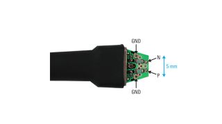
Investigating signal integrity issues requires waveforms to be sampled at locations throughout the device under test. Rohde & Schwarz supply all the necessary highspeed probes with a wide range of tips and other connectors, with high impedance and high bandwidth. The physical contact between a probe and the test point inevitably affects the electrical properties of the waveforms; Rohde & Schwarz supply functions to characterize and remove the influence of the probe from the measurements.

Benefits of our solution

Accurate and meaningful results taking account of the complete test setup. Analyze all factors reducing the signal integrity with a single instrument, with detailed analysis of both jitter and noise for the best possible insights into the causes of signal integrity problems. Highest accuracy, sensitivity and speed for phase noise analysis. A complete portfolio of general purpose test equipment providing comprehensive analysis of signal integrity issues in both the frequency and time domains, and also a wide range of general purpose and application-dependent measurments.

If you have any further questions regarding Switching Analysis, please contact us.

Related products

Related documents

Signal integrity analysis for high speed datacom interfaces

Analyzing high-speed data interfaces is crucial for signal integrity. R&S®RTP and R&S®RTO oscilloscopes with the advanced jitter option evaluate jitter and test setup impacts.

Download now

Related videos and webinars

Webinar: Effective signal fault finding: Signal Integrity verification & debugging with the R&S RTP oscilloscope

Get started on this journey to accelerate your signal integrity verification and debugging! Join the webinar to learn how to unlock the full potential of your high-speed interfaces and ensure reliable system performance.

Register now

Knowledge+

Experience the uniquely personalized, high-quality content from the whole Rohde & Schwarz ecosystem - all in a single place. Discover now our knowledge tailored for your needs.

Video center

Get access to interesting videos and webinars about solutions, applications and products.

More information

Download Center

Search the Rohde & Schwarz download center for brochures, datasheets, technical papers, manuals, firmware, software, drivers, and more.

More information

The Rohde & Schwarz Technology Academy

You’re in great hands
Practical knowledge. Industry insight. Real experts. Only with the Rohde & Schwarz Technology Academy.

More information

Sign up for our newsletter

Stay up to date on upcoming trends and latest applications.

Sign up for our newsletter

Solicitar información

¿Tiene preguntas o necesita información adicional? Simplemente complete este formulario y nos pondremos en contacto con usted.

Permiso de marketing

Se ha enviado su solicitud. Nos pondremos en contacto con usted lo antes posible.
An error is occurred, please try it again later.